


 17.03
17.03
 obd2jombang

Original TLE6208 TLE6208-3G SOP16


Car Doors And Windows Control Driver
Models : TLE6208-3g SOP16
Manufacturer : Infineon
Product Categories : Integrated Circuits (ICs), Transistor, MOSFET
Package/Case : SOP16
Reference To Part : TLE6208-3g SOP16
Substitute : TLE6208-3g SOP16
Found : Car Doors And Windows Control Driver
Package Include :
1 X TLE6208-3g SOP16
TLE6208-3g Automotive electronic IC is car engine control computer drive chip, it is easily damaged parts on Auto ECU controller board, TLE6208-3g Car engine control unit electronic IC, and the ECU Integrated Circuit IC for car electronic repair.
Three Half-Bridges
• Optimized for DC motor management applications
• Delivers up to 0.6 A continuous, 1.2 A peak current
• RDS ON; typ. 0.8 ?, @ 25 °C per switch
• Output: short circuit protected and diagnosis
• Overtemperature-Protection with hysteresis and diagnosis
• Standard SPI-Interface/Daisy chain capable
• Very low current consumption in stand-by (Inhibit)
• mode (typ. 10 µA for power and 2 µA for logic supply, @ 25 °C)
• Over- and Undervoltage-Lockout
• CMOS/TTL compatible inputs with hysteresis
• No crossover current
• Internal clamp diodes
• Enhanced power P-DSO-Package
Untuk Info barang
081332787811
Agus Yulianto
Perum Puri Astapada Indah 2 Rt:08 Rw.03 Blok K No:6
Plosogeneng Kec .Jombang, Kab.Jombang, Jawa Timur 61416
Hp. 0813-3278-7811 Kantor 0321-852845
Alamat Lokasi toko/rumah Google map
https://goo.gl/maps/7NZ4HMSYvvJ2
Web :www.obd2jombang.com
Blog
http://ToolsTeknik.blogspot.co.id
http://Obd2Jombang.blogspot.co.id
Tokopedia
https://www.tokopedia.com/obd2
Bukalapak
https://www.bukalapak.com/agusyulianto
Facebook Agus Yuli Obd Jatim
https://www.facebook.com/obd99
Rp. 90.000
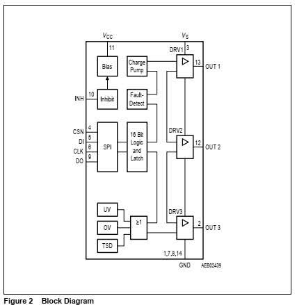
1.3 Pin Definitions and Functions
Pin No. Symbol Function
1 GND Ground; Reference potential; internal connection to pin 7, 8 and 14;
cooling tab; to reduce thermal resistance place cooling areas on PCB
close to these pins.
2 OUT3 Halfbridge-Output 3;
Internally contected to Highside-Switch 3 and Lowside-Switch 3. The
HS-Switch is a Power-MOS open drain with internal reverse diode;
The LS-Switch is a Power-MOS open source with internal reverse
diode; no internal clamp diode or active zenering;
short circuit protected and open load controlled.
3 VS Power Supply;
needs a blocking capacitor as close as possible to GND Value: 22 µF
electrolytic in parallel to 220 nF ceramic.
5 DI Serial Data Input; receives serial data from the control device; serial
data transmitted to DI is an 16bit control word with the Least
Significant Bit (LSB) being transferred first: the input has an active
pull down and requires CMOS logic level inputs;
DI will accept data on the falling edge of CLK-signal;
see Table Input Data Protocol.
4 CSN Chip-Select-Not Input; CSN is an active low input; serial
communication is enabled by pulling the CSN terminal low; CSN
input should only be transitioned when CLK is low; CSN has an
internal active pull up and requires CMOS logic level inputs.
6 CLK Serial Clock Input; clocks the shiftregister; CLK has an internal
active pull down and requires CMOS logic level inputs.
7, 8, 14 GND Ground; see pin 1.
9 DO Serial-Data-Output; this 3-state output transfers diagnosis data to
the control device; the output will remain 3-stated unless the device
is selected by a low on Chip-Select-Not (CSN);
see Table Diagnosis Data Protocol.
10 INH Inhibit Input; has an internal pull down;
device is switched in standby condition by pulling the INH terminal
low.
11 VCC Logic Supply Voltage;
needs a blocking capacitor as close as possible to GND;
Value: 10 µF electrolytic in parallel to 220 nF ceramic.
12 OUT1 Halfbridge-Output 1; see pin 2.
13 OUT2 Halfbridge-Output 2; see
 Posted in:


0 komentar:
Posting Komentar
Catatan: Hanya anggota dari blog ini yang dapat mengirim komentar.